Is there a Limit to the Chip Process Node?

Should You Believe CPU Marketing? - Process Nodes Explained
Catalog |
Is it a risk to increase the investment of advanced processes? |
Chip manufacturing process node
The core of today's integrated circuit manufacturing technology is photolithography, a method similar to photolithography in which the pattern on a mask is transferred to a silicon wafer coated with a photoresist. In the actual process, a chip is produced by dozens of photolithography sessions to complete, and some structural layers even require multiple photolithography sessions to form.
At this stage of development, the so-called physical limit is actually the wavelength limit of light, so the work done by scientists is mainly to continuously reduce the wavelength of the light used for exposure. By this method, the lithography resolution is continuously improved, and with higher resolution, more chips can be produced on the same size silicon wafer.

Chip size is getting smaller
2001: chip process node is 130nm, such as the Pentium 3 processor.
2004: the first year of 90nm.
2012: process development to 22nm. UMC, MediaTek, Ge-chip, and many other manufacturers can reach the 22nm semiconductor process.
2015: A watershed in the development of chip manufacturing, entering 14nm when UMC stopped here.
2017: Stepping into the 10nm era, Intel stopped at 10nm, and i5 and i7 processors were delayed in delivery due to yield issues.
2018: 7nm came, Intel's progress was slow, and another chip foundry giant in the United States, "Gecko", also fell at 7nm.
2019: 6nm mass production begins.
2020: the process begins to enter the 5nm era, into the more difficult 5nm, only Samsung and TSMC survived.
The status of 5nm chips
The first 5nm chip to ship is Apple's A14 Bionic chip released and marketed in October 2020, an SoC with 11.8 billion transistors, about 40% more than A13. The second is the Huawei Kirin 9000 with 15.3 billion integrated transistors.
But as semiconductor technology approaches a physical bottleneck, it is increasingly difficult to miniaturize the size of transistors. 5nm mobile chips do not seem to perform as well as they should, not only in terms of limited performance improvement but also in terms of power consumption.
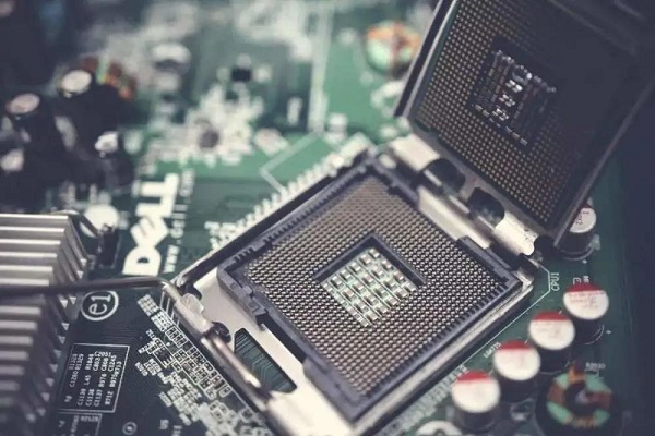
IC chip
The main reason is the immaturity of the manufacturing process, and the imbalance between the process, IC design, and power consumption. When the manufacturing process and IC design do not match, it will cause a number of problems, including power consumption, performance, etc...
Manufacturers are in pursuit of lower costs, with a smaller area of the chip, to carry more transistors. This may seem to reach the more advanced process, the better the chip performance, the lower the power consumption. But the actual situation is more complex. Some manufacturers by increasing the core, but also through the design of more complex circuitry. Whether it is to increase the core or design more complex circuitry, both need to face the problem of a power surge
In addition, the cost of 5nm chips is extremely high. Market research firm IBS gives data showing that since 28nm chip costs are rising rapidly: 28nm process costs $ 0.629 billion, to 7nm and 5nm chip costs rapidly skyrocketed, 5nm will increase to $ 476 million.
After the FinFET process, all-around gate transistors (GAA) also began to be on the agenda. TSMC originally planned to apply the technology at the 5nm node, but after taking into account the comprehensive performance and cost chose to continue to use the FinFET process. The application of GAA was postponed to the 3nm node.
2nm already in development
Although TSMC 5nm has been mass-produced, the capacity is still very limited and is still in continuous improvement. 3nm process is also expected to risk mass production in 2021 and mass production in the second half of 2022. According to Caixin news agency, TSMC recently said that it will operate an advanced production line in the new Taiwan R&D center with 8,000 engineers, and the facility will focus on researching 2nm chips and other products. Some industry voices estimate that TSMC's 2nm will be launched from 2023 to 2024.
From its birth to the present, FinEFT technology has allowed the highest breakthrough in chip process node process to 3nm. However, 3nm has almost approached the limits of FinFET. Both fin distance, short-channel effect, or materials have reached the threshold.
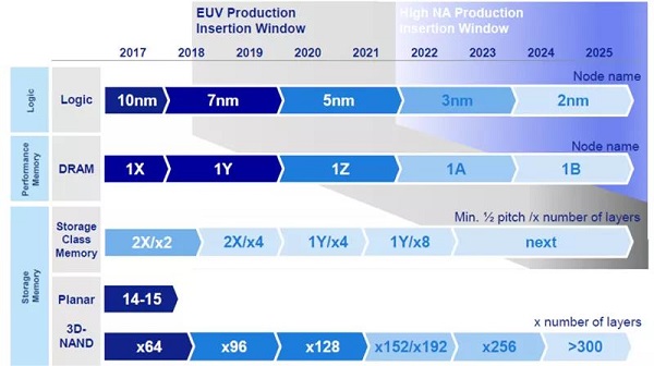
ASML forecasts semiconductor process upgrade plans
Therefore, TSMC's 2nm process with GAA technology, as an evolution of FinFET technology, can also be used to continue to suppress the short-channel effect of the technology. But in the GAA process, TSMC is not the fastest moving. TSMC will continue to follow the FinFET process on the latest 3nm process, but Samsung's 3nm has chosen the GAA process route.
GAA is an evolution of FinFET technology, which is surrounded by gates on all sides, thus once again enhancing the gate's ability to control the channel and effectively reduce leakage. It has the same concept as FinFET, with the difference that the GAA has the gate wrapped around all four sides of the channel, with the source and drain no longer in contact with the substrate.
Depending on the design, GAA also has different forms, and the four more mainstream technologies are nanowires, plate-like structure multiplexed bridging fins, hexagonal cross-section nanowires, and nanorings. The GAA technology introduced by Samsung to the public is Multi-Bridge Channel FET (MBCFET), which is a board-like structure of multiplexed bridging fins. TSMC also uses MBCFET architecture.
Process node development limits
With the further reduction of chip size, a new "physical limit" has emerged. This is the problem of our traditional computer chip design philosophy. We all know, the computer is now based on digital circuits 0, 1 such logic circuits. And as the size of the chip decreases, the smallest PN junction is also decreasing. Due to the quantum effect, the PN junction can not form the previous working state, that is, no longer exhibit such a state of 0 and 1. The quantum effect has become a roadblock for digital integrated circuits.
In fact, what is needed is not to make new PN junctions out, because PN junctions can no longer be smaller. What scientists have done is to develop the next generation of computer technology: quantum computers. This computer works differently from our current computer, which uses the quantum wave function to perform calculations. Its computational logic is different from that of digital electronic computers. The object used for quantum computing to store data is quantum bits, and it uses quantum algorithms to manipulate data.
This change is actually the process of replacing the old technical means with new ones. The new means offered by scientists in the face of digital integrated circuits that can no longer be small is quantum computing, which replaces digital computing with quantum computing and brings computing power to a new stage of development.
Currently, the chip is based on silicon. But theoretical studies show that when the chip process reaches 1nm, the quantum tunneling effect appears, that is, the electrons are not controlled. At present, human beings are compressing the performance of silicon-based materials to the limit. So the replacement of materials has been on the agenda, the most promising is molybdenum disulfide (MoS2).
Both silicon and molybdenum disulfide has a crystal structure, but molybdenum disulfide is stronger than silicon for controlling electrons. As we all know, the gate of the transistor is responsible for the flow of electrons, playing the role of the switch. At the 1 nm node, the gate is difficult to play its role. By molybdenum disulfide, this problem will be solved, and the dielectric constant of molybdenum disulfide is very low, which can be compressed to a 1nm gate.
Is it a risk to increase the investment of advanced processes?
Currently, the performance and power returns of chips brought by advanced processes are being significantly reduced. In recent months, smartphones equipped with 5nm process SOCs have been released one after another. From the actual performance of these phones, whether TSMC's 5nm FinFET process or Samsung's 5nm LPE process, performance, power consumption improvements have failed to meet market expectations.
Samsung: the problem of power consumption is more prominent. Compared with the previous generation of Snapdragon 865 processors, Snapdragon 888 processor’s single-core power consumption and multi-core power consumption increased significantly, the energy efficiency performance dropped significantly.
TSMC: Apple A-series processors, for example, also based on TSMC 7nm process, A13 processor compared to A12 processor CPU performance increased by 20%, GPU performance increased by 20%. Compared to the A13, the A14, which is based on TSMC's 5nm process, has a CPU performance improvement of about 16.7% and a GPU performance improvement of about 8.3%.
In other words, in Apple's A-series processors, the progress brought by the 5nm process advancement is likely to be less than Apple's own optimization and upgrade of the processor architecture. Although there is some industry speculation that this is due to the 5nm initial yield rate is not high, Apple A14 shielded some cores. However, the Kirin 9000, which also uses TSMC's 5nm process, also has a large difference in power control compared to the official data.
The actual performance of the 5nm advanced process is generally not satisfactory, and the marketing value of the products using the 5nm process at this stage may far exceed the practical value of the advanced process itself.
What is even more disturbing is that TSMC is continuing to increase its R&D investment in the next-generation process node, the 3nm process, when the practical value of TSMC's 5nm process is very much in question. In the recent earnings meeting, TSMC management announced plans for 2021 to significantly increase annual capital expenditures from $17 billion in 2020 to $25 billion to $28 billion, an increase of 45% to 63%, of which about 80% will be used for 3nm process research and development, which means that TSMC will have more than $15 billion in capital expenditures to 3nm process this year.
According to TSMC's previously announced plan, their 3nm process, planned for risky trial production this year, large-scale mass production in 2022. In other words, according to TSMC's plan, we can see some products equipped with TSMC's 3nm process in the market next year.
This is still in line with TSMC's advanced process upgrade rhythm in recent years, however, from the actual performance of the product, the high cost has not perfectly achieved the expected results. In other words, TSMC has probably hit a bottleneck between capital investment and technology implementation. Ignoring this bottleneck and eagerness to achieve the 3nm advanced process, TSMC has actually fallen into an extreme technology adventure.
1.What is a technology node?
A term used in semiconductor device fabrication to describe the size of the features in the finished product. Quoted in terms of nanometres (or larger for earlier nodes), the node name refers to half the distance between identical features in a memory cell.
2.Is 1 nm chip possible?
Present-day technology already has the capability to produce chips down to the 3-nm scale, with production by TSMC slated to start in the second half of 2022. This 1-nm node breakthrough could potentially break the limits of Moore's Law.
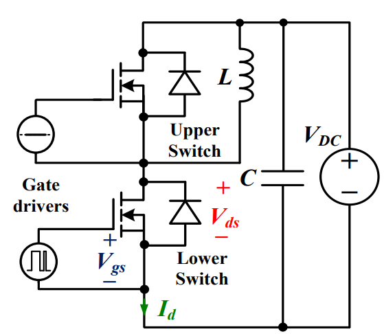 Discovering New and Advanced Methodology for Determining the Dynamic Characterization of Wide Bandgap DevicesSaumitra Jagdale15 March 20242508
For a long era, silicon has stood out as the primary material for fabricating electronic devices due to its affordability, moderate efficiency, and performance capabilities. Despite its widespread use, silicon faces several limitations that render it unsuitable for applications involving high power and elevated temperatures. As technological advancements continue and the industry demands enhanced efficiency from devices, these limitations become increasingly vivid. In the quest for electronic devices that are more potent, efficient, and compact, wide bandgap materials are emerging as a dominant player. Their superiority over silicon in crucial aspects such as efficiency, higher junction temperatures, power density, thinner drift regions, and faster switching speeds positions them as the preferred materials for the future of power electronics.
Read More A Comprehensive Guide to FPGA Development BoardsUTMEL11 September 202515960
This comprehensive guide will take you on a journey through the fascinating world of FPGA development boards. We’ll explore what they are, how they differ from microcontrollers, and most importantly, how to choose the perfect board for your needs. Whether you’re a seasoned engineer or a curious hobbyist, prepare to unlock new possibilities in hardware design and accelerate your projects. We’ll cover everything from budget-friendly options to specialized boards for image processing, delve into popular learning paths, and even provide insights into essential software like Vivado. By the end of this article, you’ll have a clear roadmap to navigate the FPGA landscape and make informed decisions for your next groundbreaking endeavor.
Read More Applications of FPGAs in Artificial Intelligence: A Comprehensive GuideUTMEL29 August 20253881
This comprehensive guide explores FPGAs as powerful AI accelerators that offer distinct advantages over traditional GPUs and CPUs. FPGAs provide reconfigurable hardware that can be customized for specific AI workloads, delivering superior energy efficiency, ultra-low latency, and deterministic performance—particularly valuable for edge AI applications. While GPUs excel at parallel processing for training, FPGAs shine in inference tasks through their adaptability and power optimization. The document covers practical implementation challenges, including development complexity and resource constraints, while highlighting solutions like High-Level Synthesis tools and vendor-specific AI development suites from Intel and AMD/Xilinx. Real-world applications span telecommunications, healthcare, autonomous vehicles, and financial services, demonstrating FPGAs' versatility in mission-critical systems requiring real-time processing and minimal power consumption.
Read More 800G Optical Transceivers: The Guide for AI Data CentersUTMEL24 December 20254728
The complete guide to 800G Optical Transceiver standards (QSFP-DD vs. OSFP). Overcome supply shortages and scale your AI data center with Utmel Electronic.
Read More The 2026 Engineer’s Guide: Choosing the Right MCU for Your Next IoT & New Energy ProjectUTMEL30 April 202668
A comprehensive comparison of 2026's leading MCUs from ST, NXP, and Microchip across power efficiency, processing performance, connectivity, and ecosystems to help engineers select the optimal chip for next-gen IoT and new energy projects.
Read More
Subscribe to Utmel !
![ATSHA204A-MAHDA-S]() ATSHA204A-MAHDA-S
ATSHA204A-MAHDA-SMicrochip Technology
![HCS360-I/SN]() HCS360-I/SN
HCS360-I/SNMicrochip Technology
![AT88SC0204CA-SH]() AT88SC0204CA-SH
AT88SC0204CA-SHMicrochip Technology
![CS8190EDWFR20G]() CS8190EDWFR20G
CS8190EDWFR20GON Semiconductor
![ATECC608A-MAHDA-T]() ATECC608A-MAHDA-T
ATECC608A-MAHDA-TMicrochip Technology
![ATSHA204A-MAHCZ-T]() ATSHA204A-MAHCZ-T
ATSHA204A-MAHCZ-TMicrochip Technology
![HCS301/SN]() HCS301/SN
HCS301/SNMicrochip Technology
![AT88SC0808CA-Y6H-T]() AT88SC0808CA-Y6H-T
AT88SC0808CA-Y6H-TMicrochip Technology
![ATAES132A-SHEQ-T]() ATAES132A-SHEQ-T
ATAES132A-SHEQ-TMicrochip Technology
![HCS201-I/P]() HCS201-I/P
HCS201-I/PMicrochip Technology


 Product
 Brand
Brand Articles
 Tools
Tools


